In modern semiconductor manufacturing, the path from wafer fabrication to finalized integrated circuit (IC) packaging demands uncompromising electrical testing. Wafer probing (also known as Chip Probe (CP) or Wafer Sorting) serves as the primary barrier preventing defective dies from proceeding to expensive packaging stages. As design nodes shrink toward 3nm and below, the density of pad layouts increases exponentially. This micro-scale progression places massive stress on the electrical interfaces connecting the wafer's pads to the Automated Test Equipment (ATE).
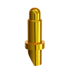
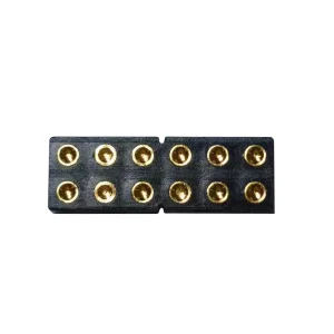
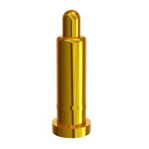
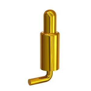
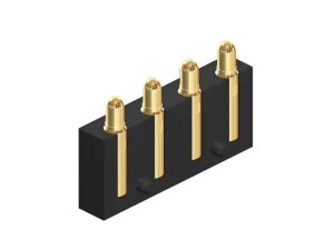
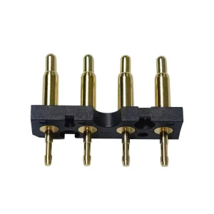
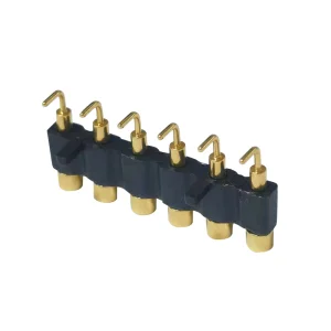
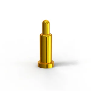
For procurement managers and hardware design engineers, finding a cost-effective wafer testing manufacturer or factory is not simply about seeking the lowest unit cost. It represents a multidimensional optimization of contact lifetime, impedance stability, signal integrity, and lead times. The primary mechanical interface inside test sockets and vertical probe cards is the spring-loaded contact pin (Pogo Pin). Precision pogo pins provide the dynamic compliance necessary to absorb wafer coplanarity variances, guaranteeing reliable, low-resistance connections during multi-site high-throughput testing cycles.
| Testing Parameter | Technical Challenge | Pogo Pin Interface Solution | Impact on Wafer Test Yield |
|---|---|---|---|
| Contact Resistance (Cres) | Oxide layers build up on wafer pads, causing erratic measurements. | Customized gold-plated tips with tailored spring force (e.g., >15g) to pierce oxides. | Reduces false failures (overkill), keeping yield measurements highly accurate. |
| High Frequency / RF | Signal degradation at high frequencies (5G, automotive radar, WiFi 6E/7). | Extremely short pogo pin designs with matched impedance characteristics. | Allows accurate parametric evaluation of high-speed RF ICs at wafer level. |
| Pitch Scaling | Shrinking pad size down to micro-pitches (<0.4mm). | Ultra-miniaturized SMT probe pins with precise cylindrical tolerancing. | Supports high-density multi-die parallel test architectures. |
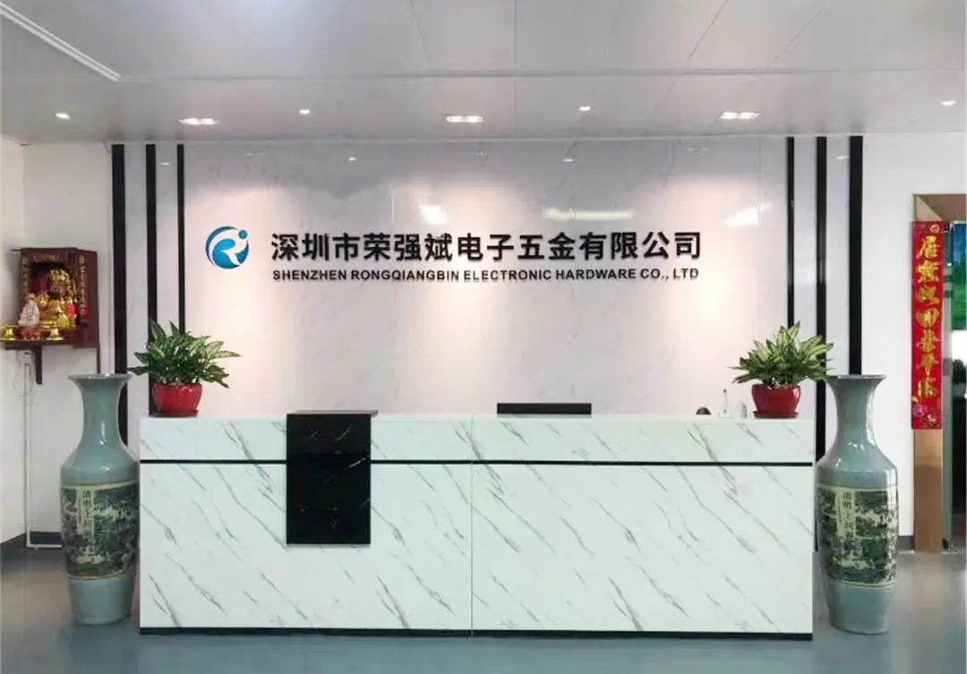
Shenzhen Rongqiangbin Electronic Hardware Co., Ltd. is strategically located in Shenzhen, the leading city of the Guangdong-Hong Kong-Macao Greater Bay Area. Founded in February 2011 on Songgang Street, Shenzhen, our company has dedicated over a decade to the advanced engineering, development, and high-volume manufacturing of high-performance Pogopin connectors and spring-loaded probing interfaces.
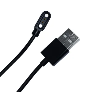
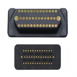
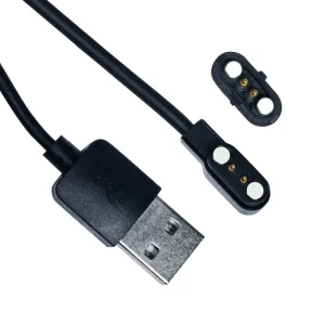
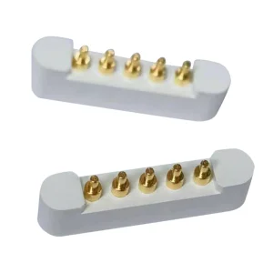
Through continuous technological refinement, process automation, and intense physical metallurgy research, Rongqiangbin has transitioned from a localized component workshop into an internationally recognized industry pioneer. We provide key contact systems for complex testing configurations, spring contacts, and magnetic modular interfaces.
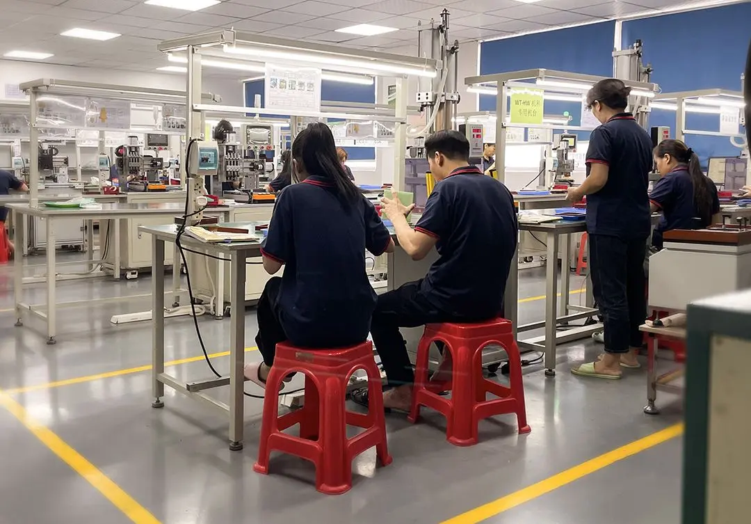
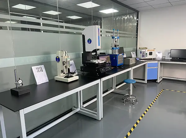
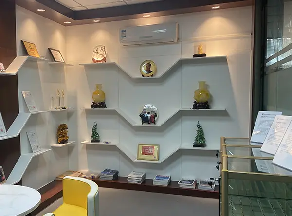
Our operational ethos—"customer first, integrity first"—is backed by our registration and compliance with the ISO9001:2015 international quality management system certification. Our production facility leverages state-of-the-art Japanese CNC machining equipment, dynamic loading testers, and micro-resistance analysis setups to satisfy the most stringent global quality standards.
"Committed to being an excellent POGO PIN manufacturer for both quality and cost on home and abroad, and leading connector technology development." We actively bridge the gap between expensive testing instrumentation and cost-competitive component supply chains.
Our precision-manufactured pins and assemblies are trusted by market-leading organizations including: Honeywell, Samsung, SIEMENS AG, ZTE, 360, QCY, HAYLOU, Shanghai Laimu, Luxshare Group, Aoni Electronics, and Amphenol Group.

How we balance highly competitive cost structures ("cheap" manufacturing) with elite technical excellence.
Over a decade of dedication to pogo pin physics. Our expert engineers understand force-deflection dynamics, spring fatigue, and mechanical cycles.
Every batch undergoes automated optical inspection (AOI) and comprehensive electrical testing. We guarantee zero-defect shipments.
Equipped with X-ray thickness testers, spring force testers, contact resistance analyzers, and high-frequency network analysis platforms.
As integrated circuits move deeper into sub-micron territories, wafer testing interfaces encounter extreme technical boundaries. High-density system-on-chip (SoC) architectures and multi-chip high-bandwidth memory (HBM) stacks require test pins that can handle massive electrical currents in increasingly miniature form factors.
Rongqiangbin is actively investing in new surface treatment methods to extend the operational lifetime of testing interfaces. By applying optimized gold alloys and anti-friction platings, we reduce the accumulation of aluminum debris on probe tips. This reduces cleaning intervals and keeps contact resistance extremely low over millions of test cycles.
At the same time, we are adapting our production lines to support the integration of vertical probe cards. This mechanical upgrade ensures that testing assemblies are fully prepared for the upcoming transition from traditional chip probes to high-frequency vertical testing platforms.
When searching for a cheap wafer testing manufacturer, high-volume procurement teams often worry about risking quality. At Rongqiangbin, we have spent years optimizing our operations to prove that cost-efficiency and technical quality can go hand-in-hand. We achieve this balance by embracing modern Industry 4.0 principles, automating production, and capitalizing on the industrial advantages of Shenzhen's hardware manufacturing ecosystem.
We use high-precision CNC automatic turning centers to turn raw brass and beryllium copper alloys into micro-pins with micron-level accuracy. Automated machining reduces human error and maximizes material yield.
Operating from Songgang Street in Shenzhen connects us directly to the world's most complete hardware supply chain. We procure raw materials, complete surface platings, and coordinate air shipments with minimal transit time.
We design and refine our tooling molds completely in-house. This capability cuts ODM prototyping costs down to a fraction of traditional third-party rates, and reduces customization time to a few working days.
Our spring contacts and high-reliability testing connectors are tailored for diverse industrial ecosystems.
Automotive grade testing requires absolute stability across a wide temperature range. We utilize high-durability alloys and gold-plated surfaces to prevent contact degradation under mechanical shock and thermal cycling.
For RF testing in wireless and portable consumer products, our low-inductance pogo pins deliver exceptional signal integrity up to several gigahertz. This ensures fast, reliable parametric wafer sorting.
Global supply chain managers must balance price considerations with total cost of ownership (TCO). Unplanned production downtimes or test card failures due to unreliable probe pins can quickly erase any savings achieved on initial component purchase prices.
All raw metal components—including copper wire, beryllium copper alloys, and stainless steel springs—are sourced with complete material mill sheets and chemical analysis reports to guarantee structural integrity.
Rongqiangbin guarantees that all manufacturing processes are fully compliant with RoHS and REACH regulations. We eliminate hazardous heavy metals from our finishes to ensure environmental compatibility.
Our engineering team works directly with client hardware and test engineers. By reviewing Gerber files, pin maps, and mechanical clearance plans early in the process, we eliminate costly design mistakes.
Critical technical insights for semiconductor test engineers and procurement specialists.
 Rongqiangbin Electronic