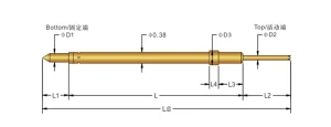
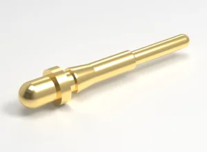
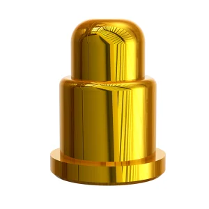
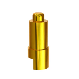
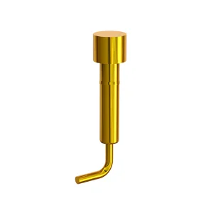
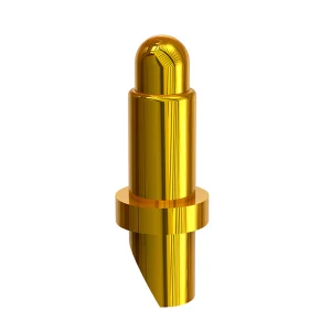
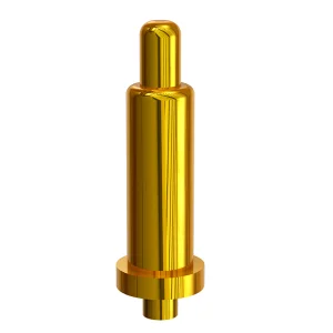
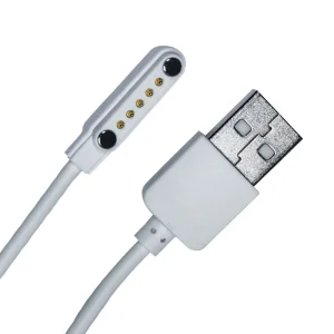
In the high-stakes ecosystem of semiconductor validation, RF circuit design, and telecommunications testing, high frequency testing needles (often structurally formulated as coaxial RF probes, high-speed spring-loaded contacts, or high-bandwidth probe card pins) serve as the vital electrical bridge. Unlike conventional low-frequency pogo pins, high-frequency testing needles must preserve signal integrity at frequencies stretching from 10 GHz to over 80 GHz.
To prevent signal degradation, these probes are engineered to maintain a strict 50Ω or 75Ω characteristic impedance match across the path. The electrical continuity, insertion loss (S21), and return loss (S11) must be meticulously calibrated. Any structural variation at the micro-millimeter scale will cause capacitance or inductance shifts, leading to critical signal reflection and false negatives during IC production tests.
Maintained via precise internal shielding and dielectric isolation. Crucial for RF coaxial testing, limiting signal attenuation in 5G and radar transceiver chips.
Micro-fabricated designs allowing contact spacing down to 0.2mm, meeting the shrinking geometries of modern high-density wafer packaging.
Leveraging aerospace-grade spring materials (such as Music Wire or Beryllium Copper alloys) for high mechanical resiliency and stable contact forces.
As the international electronic manufacturing and testing sector changes, China-based manufacturers have moved up the value chain from basic assembly to precision micro-machining and advanced RF component engineering. Companies located in high-tech industrial hubs—specifically the Guangdong-Hong Kong-Macao Greater Bay Area (Shenzhen, Dongguan)—provide structural benefits that global procurement managers rely on:
By centering manufacturing operations within Shenzhen, factories enjoy immediate proximity to premium brass, beryllium copper, PEEK, and Teflon insulators. Micro-electroplating facilities nearby allow for rapid iterations of plating thicknesses, ensuring short lead times for customized RF probes.
Chinese OEM/ODM developers have heavily integrated Swiss-type automatic lathes, CNC micromachining tools, and automated visual sorting inspection lines. This high level of automation reduces dimensional variation to within ±0.005mm, preventing mechanical misalignments in multiconductor wafer test probes.
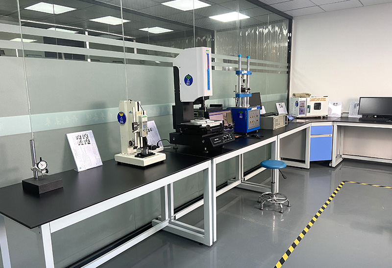
With standardized factories ISO9001:2015 certified, manufacturing operations align with international reliability standards. Inspection equipment includes X-ray fluorescence (XRF) for plating thickness, vector network analyzers (VNA) for S-parameter matching up to 40GHz, and high-speed mechanical fatigue testers.
Evaluating cost-to-performance metrics shows why Global 500 tech companies source their customized components from high-frequency testing needle factories in Shenzhen:
| Metric | Shenzhen (RQB) | Euro/US Brands |
|---|---|---|
| Lead Time | 5 - 10 Days | 4 - 8 Weeks |
| Custom Setup | Flexible MOQ | High Entry Barrier |
| Direct Tech Support | 24/7 Engineer Access | Layered Helpdesks |
| Material Cost | Highly Cost-Effective | Premium Markup |
Precision high-frequency testing needles are designed for diverse, demanding environments. They play an essential role in quality assurance, lab validation, and batch production protocols across several key industries:
Testing telecommunication transceivers, MIMO antennas, and power amplifiers requires RF probes that support frequencies exceeding 28GHz. High-frequency needles allow for repeatable, automated over-the-air (OTA) testing interfaces, maintaining stable 50Ω impedance to ensure clear diagnostic results during high-speed production runs.
Modern Advanced Driver Assistance Systems (ADAS) depend on millimeter-wave radar modules. Characterization and production testing of these radar chips demand highly durable coaxial testing needles. They must operate under thermal extremes (-40°C to +125°C) inside climatic chambers while delivering low-noise RF signal transmission.
As microchip packaging moves toward chiplets and high-density system-in-packages (SiP), pin pitches continue to shrink. In ATE (Automated Test Equipment) setups, our micro-pitch pogo probes ensure clean electrical contact on wafer pads. This allows for high-throughput parametric testing of logic, memory, and RF chips.
The transmission speeds of modern physical layer interfaces have reached up to 40Gbps per lane. Evaluating these high-speed serial links on consumer mainboards requires testing needles that minimize jitter, crosstalk, and signal insertion losses. This helps guarantee consistent physical layer compliance testing.
Shenzhen Rongqiangbin Electronic Hardware Co., Ltd. is strategically located in Shenzhen, the leading technology and industrial manufacturing city of the Guangdong-Hong Kong-Macao Greater Bay Area. Founded in February 2011 on Songgang Street, Shenzhen, the company has focused on the engineering, development, and high-precision manufacturing of Pogo Pin Connectors. After years of dedicated research and quality improvement, the company has become a trusted developer in the custom probe and connector industry.
Our corporate culture centers on the principle of "customer first, integrity first." We have built a skilled, collaborative production team with deep technical expertise in the Pogo Pin industry. This foundation has allowed us to establish long-term partnerships with leading companies worldwide. To guarantee high quality, Rongqiangbin has secured the ISO9001:2015 international quality management system certification. Backed by a strict quality assurance team and environmental management systems, we ensure all products comply with RoHS and REACH environmental guidelines.
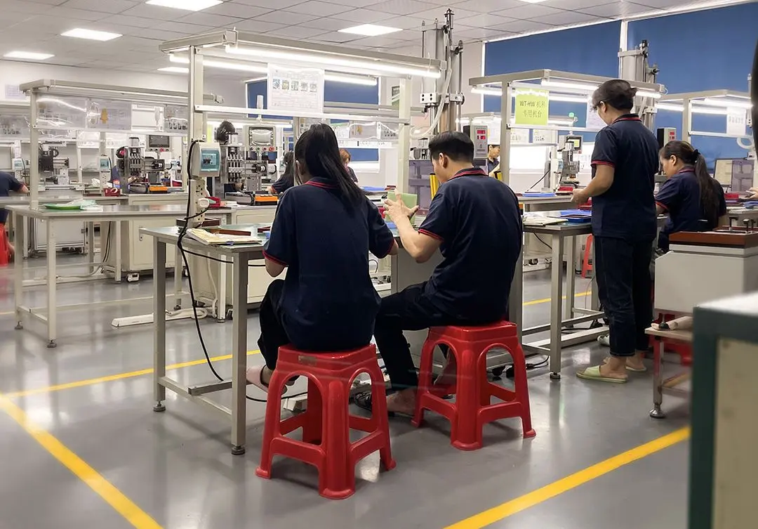
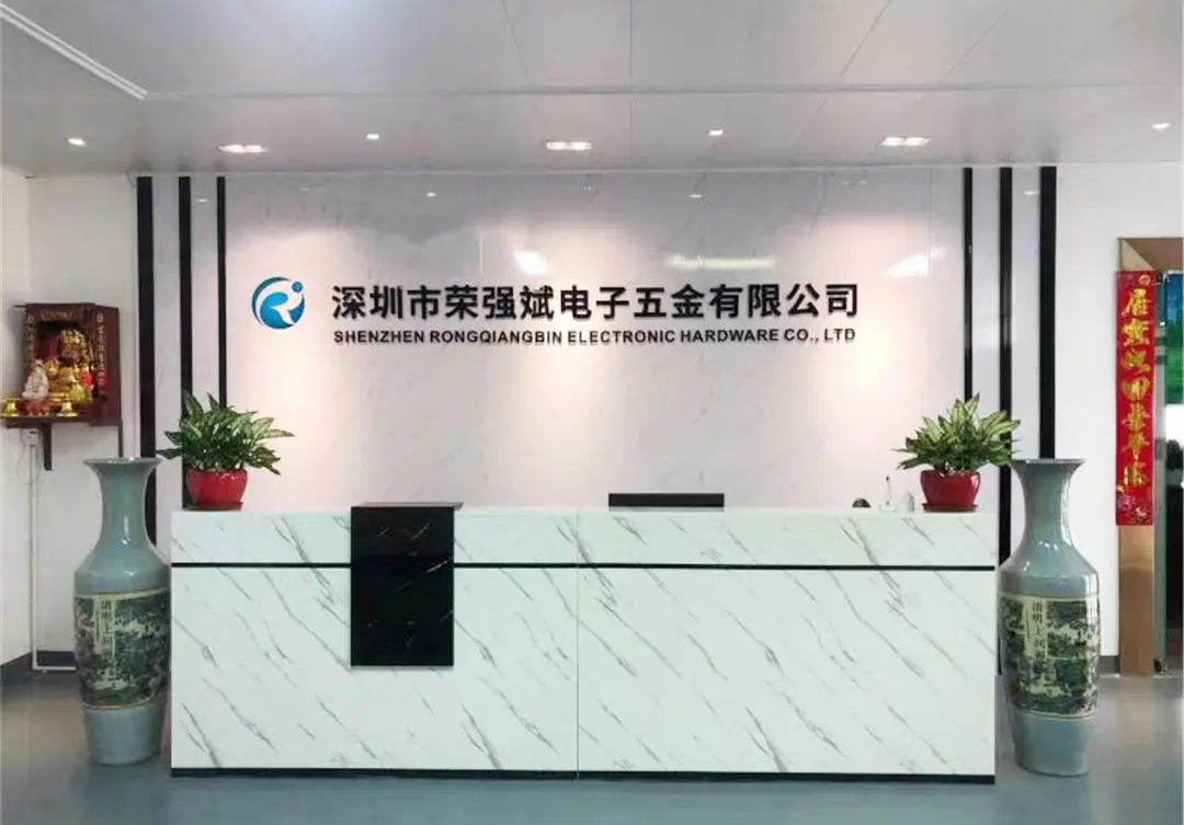

"Committed to being an excellent POGO PIN manufacturer for both quality and cost on home and abroad, and leading connector technology development."
We work to lower cost barriers while maintaining strict quality metrics. This helps global technology developers access precision connection interfaces without compromising design speed or product durability.
By investing in in-house research and development, we have secured over 300 patents. This IP portfolio covers structural spring designs, low-resistance plungers, high-current transmission contacts, and specialized high-frequency testing needles.
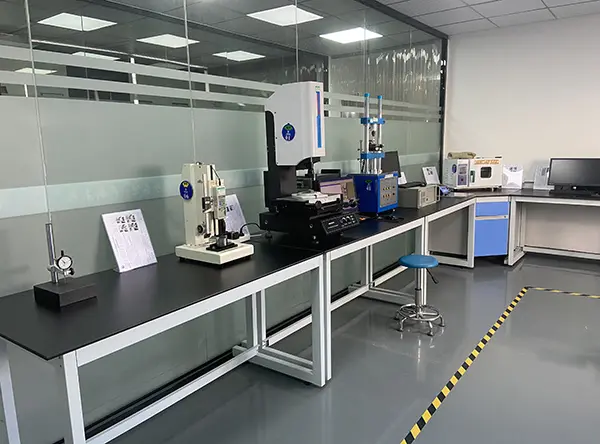
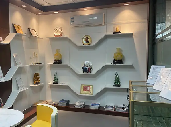

As global industries transition toward artificial intelligence, autonomous driving, and high-performance computing (HPC), testing requirements are undergoing shifts:
Next-generation system-on-chip designs require probe systems that can contact micro-bumps spaced less than 150 microns apart without causing cross-talk or mechanical damage.
Modern testing heads need to transmit high-speed RF, optical, and high-power currents simultaneously. High-frequency needles are co-engineered alongside high-current contacts to prevent thermal interference.
Using HFSS software for 3D electromagnetic simulations has become standard. Probes are pre-simulated and matched to their exact target board layouts to minimize return loss (S11) anomalies before manufacturing.
A standard pogo pin is designed to handle direct current or low-frequency signals and does not have impedance control. In contrast, a high-frequency testing needle features a coaxial configuration. It includes a central conductor, a dielectric insulator (such as PTFE or PEEK), and an outer shielding barrel. This design maintains a stable impedance (e.g., 50 Ohm), which helps prevent signal reflection and high attenuation during RF testing.
Gold (Au) offers excellent electrical conductivity and high resistance to oxidation and corrosion. Plating the plunger and inner barrel with gold ensures a stable, low contact resistance. Additionally, it helps maintain mechanical durability over hundreds of thousands of compression cycles, which is critical for consistent testing results.
We use high-precision CNC lathe machining to maintain tolerances within ±0.005mm. During testing, we utilize vector network analyzers (VNA) to measure S-parameters, checking both insertion loss and return loss. Every product batch undergoes rigorous testing before shipment to verify that electrical performance matches the specifications.
Plungers are commonly made from SK4 (tool steel) or Beryllium Copper (BeCu). SK4 is chosen for its high hardness, making it ideal for sharp tips that need to pierce oxidation layers on solder pads. Beryllium Copper is selected for its excellent balance of electrical conductivity, mechanical elasticity, and resistance to fatigue.
Yes, customization is a core part of our business. With over 10 years of manufacturing experience, we can customize probe dimensions, spring forces, tip geometries, and impedance characteristics to meet your specific electrical and mechanical requirements.
 Rongqiangbin Electronic