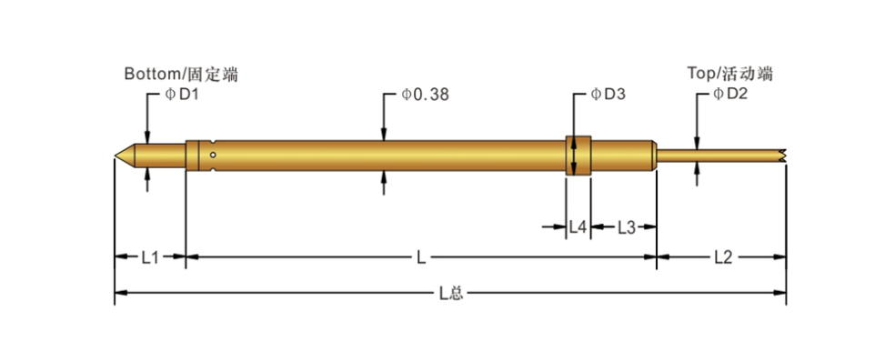
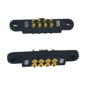
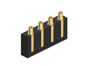
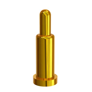
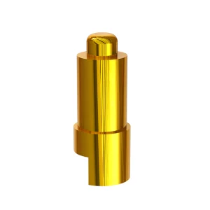
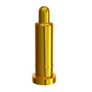
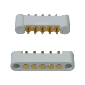
SCFB038 Series
ProductParameters
Materials & Plated:
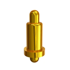
Needle Tube (Barrel): Ph, Au on Ni Plated
Needle 1 (Plunger): SK4/Becu, Auon Ni Plated; PD, No PlatedNeedle 2 (Plunger): SK4/Becu, Au on Ni Plated; PD,No PlatedSpring (Spring): SWP /SUS, Au on Ni Plated
Electrical Specifications:
Frontal Static Current (Current Rating): 3 Amps
Bandwidth: -1 dB @ 13.1 GHzInductace (Inductace):1.20 nHCapacitance:1.55 pF
ProductIntroductior
nign est ctort ehen n ltucuranl ae d. auarea mingl ao rbe cnel uon ad doube ation pro esth eml volume and
Mainly used for extremely low contact resistance and utra -high bandwidth in various communication power electronic components,semiconductor wafer
testing, chip packaging testing, etc, meeting requirements for 5-40G high-frequency signal testing.
Currently, Xindeli can process small probe diameter: head p: 0.06 mm / needle tube q: 0.10 mm.
Semiconductor test probes are also known as "dual head probes". Commonly used internal needle types include B, J1, U, U1, etc., featuring small sizes and meeting high testing accuracy requirements.
Structural Classification
Dual-head - single-action probe series
Dual-head - double-action probe series
Key Applications
Semiconductor wafer testing
Chip packaging testing
Communication power electronic components
Technical Specifications & Capabilities
These probes are mainly used for achieving extremely low contact resistance and ultra-high bandwidth, fully meeting the requirements of 5-40GHz high-frequency signal testing.
Currently, small probe diameters can be processed down to: Head 0.06mm / Needle tube φ 0.10mm.
Frequently Asked Questions (FAQ)
1. What are semiconductor test probes also known as?
Semiconductor test probes are also commonly referred to as "dual head probes".
2. What are the common internal needle types for these probes?
The commonly used internal needle types include B, J1, U, and U1. They are designed for small size and high testing accuracy requirements.
3. How are the probe structures categorized?
They are structurally divided into two main series: the dual-head - single-action probe series and the dual-head - double-action probe series.
4. What are the primary testing applications for these probes?
They are mainly used for semiconductor wafer testing, chip packaging testing, and testing various communication power electronic components.
5. What frequency range can these semiconductor test probes support?
They are engineered to meet the requirements of 5-40GHz high-frequency signal testing, offering extremely low contact resistance and ultra-high bandwidth.
6. What is the minimum probe diameter size that can be processed?
The minimum processable small probe diameters are a head size of 0.06mm and a needle tube diameter of φ 0.10mm.
 Rongqiangbin Electronic