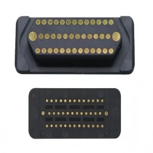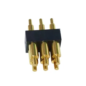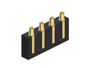
High-Quality High Current Probes Supplier & Factory

Precision Engineering & Thermal Management for High-Power Semiconductor, Battery, and Automotive Test Interfaces

High Current Probes: Engineering the Future of Power Testing

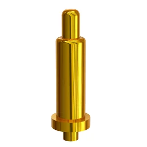
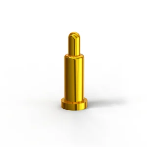
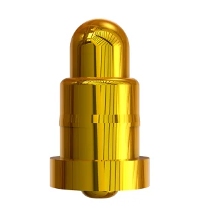
In the contemporary electrical test and measurement landscape, the paradigm is rapidly shifting toward higher currents, minimized resistance, and prolonged lifecycle profiles. High Current Probes—specialized spring-loaded contacts engineered to bridge test instruments and active circuits under high electrical load—play an indispensable role in assuring accuracy, component safety, and process repeatability.

As microelectronics scale down and electric drivetrains scale up, testing interfaces must endure severe conditions. High current probes mitigate critical failure modes, including excessive thermal heating, high contact resistance, and premature fatigue. Integrating high current design principles within automated test environments (ATE) dictates the yield rate of production lines globally.

Key Mechanical & Metallurgical Pillars

  • Optimized Plunger Metallurgy: Beryllium Copper (BeCu) or Tellurium Copper (TeCu) alloys are selected for their supreme balance of electrical conductivity and structural tensile strength.
  • Advanced Multi-layer Plating: Gold-over-nickel plating ensures minimized contact resistance (< 10 mΩ) while offering resilience against atmospheric oxidation and repeated cycling wear.
  • Custom Spring Dynamics: Tailored spring forces prevent indentation on delicate target pads while providing sufficient penetration through surface oxide films.
Global Industrial Landscape & Commercial Imperatives

Evaluating market forces and shifting demands across the electronic testing, battery assembly, and electric vehicle sectors.

EV Battery Formation & Testing

Modern lithium-ion cells require massive charging currents during formation stages (often exceeding 50A to 100A per cell). High-current contact probes must sustain continuous electrical loads without causing temperature spikes that could trigger thermal runaway or degrade the cell chemistry.

Power Semiconductor Testing

The proliferation of Silicon Carbide (SiC) and Gallium Nitride (GaN) high-power semiconductor modules requires high current test interfaces that operate at elevated temperatures. High current probes ensure steady, zero-bounce contact during wafer-level and packaged-device characterization.

Automated Assembly Lines

In Smart Factories, automated testing cycles operate 24/7. High reliability is crucial; a probe line failure can stop output immediately. Durability and ease of quick-change maintenance are core components of lower total cost of ownership (TCO).

The rapid deployment of fast-charging infrastructures and renewable energy storage systems highlights the need for robust test contacts. Suppliers must focus on customized designs tailored to target surface geometries and environmental variables.

Technology Roadmap & Engineering Futures

Deep dive into materials science, coating systems, and micro-electromechanical architectures shaping the next generation of testing probes.

Performance Parameter Current Market Standards Next-Generation (RQB Roadmap) Core Technical Enabler
Continuous Current Capacity 15A - 30A 50A - 150A+ Direct coax internal bypass design, customized solid copper plungers.
Typical Contact Resistance < 20 mΩ < 5 mΩ Multi-contact point crown heads & hyper-dense gold alloy coatings.
Mechanical Lifecycle 100,000 to 300,000 cycles 1,000,000+ cycles Premium spring steel alloys with enhanced fatigue limit & smooth barrel interiors.
Operational Temp. Limit -40°C to 120°C -55°C to 180°C+ HT-grade stainless steel springs & specialized heat dissipation shrouds.

1. Coaxial Flow & Hybrid Designs

By separating high current pathways from the internal spring structure, modern probes bypass the spring to prevent localized inductive heating. This maintains spring integrity over hundreds of thousands of cycles.

2. Innovative Surface Coatings

We utilize hard gold plating over high-barrier nickel diffusion layers. This ensures sustained low contact resistance even in environments prone to chemical off-gassing and elevated humidity.

3. Miniature High Current Interfaces

Consumer wearables and high-density computing platforms demand compact form factors. Modern R&D centers on building high current-carrying capacity within sub-1.0mm pitch envelopes.

Shenzhen Rongqiangbin Electronic Hardware Co., Ltd.

Located in Shenzhen, the leading city of the Guangdong-Hong Kong-Macao Greater Bay Area, our company was founded in February 2011 in Songgang Street, Shenzhen. We specialize in the design, development, and high-volume manufacturing of high-performance Pogopin connectors and high-current spring probe systems. Through years of research, technical accumulation, and production improvements, the company has become a leader in the precision connector industry.

Guided by the principle of "customer first, integrity first", Rongqiangbin boasts a strong POGO PIN industry technology production team and long-term partnerships with leading global enterprises. We have obtained the ISO9001:2015 version of the international authoritative quality management system certification, supported by a robust quality control team and environmental management system to deliver high-quality, eco-friendly products.

Our Vision: Committed to being an excellent POGO PIN manufacturer for both quality and cost, at home and abroad, and leading connector technology development.

Our Global Client Portfolio

We are a trusted supply chain partner to leading enterprises, including Honeywell, Samsung, SIEMENS AG, ZTE, 360, QCY, HAYLOU, Shanghai Laimu, Luxshare Group, Aoni Electronics, and Amphenol Group.

Why Choose Us

  • 01
    10+ Years of Manufacturing Experience

    Partnered with 4000+ global clients and holding 300+ structural patents.

  • 02
    Perfect Quality System Certification

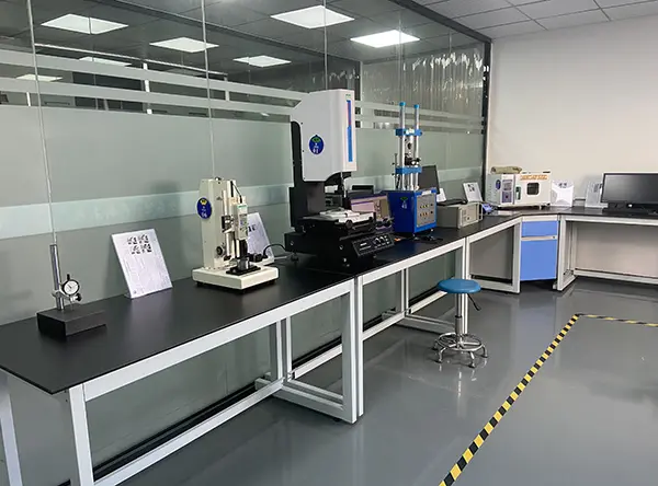
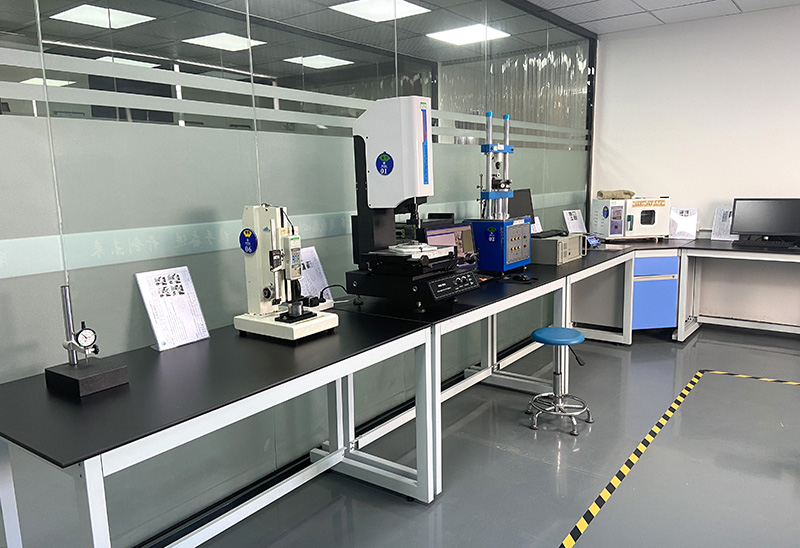
    ISO9001:2015 certified plant with advanced testing instruments.

  • 03
    100% Inspection Protocols

    Rigorous checks in production and before shipping to guarantee zero failures.

  • 04
    Fast Delivery & After-Sales Support

    Efficient lead times and quick technical response.

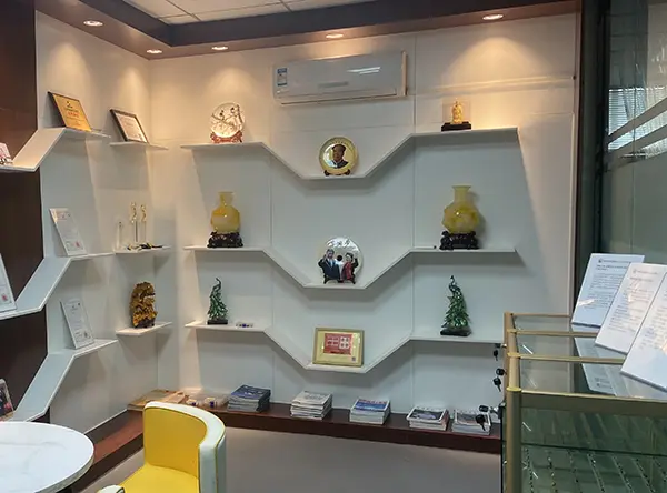
Patent Certificate 1 Patent Certificate 2

10+

Years in Production

4000+

Global Clients

300+

Connector Patents

100%

Quality Checked

Macro-Industry Solutions & Customization

How RQB connector designs solve structural, thermal, and mechanical electrical constraints in modern test interfaces.

Thermal analysis

High Current Thermal Simulation

We perform Finite Element Analysis (FEA) to map thermal profiles. Understanding heat generation at high current loads allows us to optimize geometries, ensuring stability at 150°C+ ambient temperatures.

Plating control

Surface Plating Verification

Using X-Ray Fluorescence (XRF) and automated cross-section analyzers, we verify plating thickness at deep micro-cavities of barrels, assuring lasting oxidation defense under critical cycles.

R&D

Custom Structural Engineering

We tailor plunger tips (waffle, cup, crown, point, flat) to match target contact pads, minimizing surface deformation while maximizing electrical contact area.

Technical Q&A & Search Intent Insights

Deep engineering answers addressing common questions regarding high current probe implementation, reliability, and custom pogo connector design.

What is the primary factor limiting the current-carrying capacity of a spring probe?

The current-carrying capacity of standard spring probes is primarily limited by the internal resistance of the spring. Because steel or beryllium copper springs have small cross-sectional areas and high resistance relative to solid copper, running high currents directly through the spring causes excessive Joule heating ($I^2R$). This heating can detemper the spring, resulting in lost spring force and mechanical failure. Modern high-current probes resolve this by utilizing a bias-cut plunger or internal coaxial insulation, channeling current through a highly conductive barrel and plunger instead of the spring.

How does RQB control quality during high-volume production?

At Shenzhen Rongqiangbin, we operate under ISO9001:2015 guidelines. Quality is maintained through a combination of automated optical inspection (AOI), dynamic spring force displacement profiling, contact resistance measurement under actual working compression states, and precise X-ray validation of plating thickness. We perform a 100% inspection protocol on critical tolerances before packaging and shipping.

Why is gold over nickel plating preferred for industrial high current pins?

Gold is highly conductive and does not form oxides under atmospheric conditions, ensuring low and repeatable contact resistance. The nickel underplate acts as a diffusion barrier, preventing copper atoms from migrating to the gold surface and oxidizing. It also provides mechanical support to the soft gold layer, improving overall wear resistance.

Can you provide custom magnetic assemblies containing pogo pins?

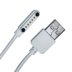
Yes, custom ODM and OEM magnetic charging interfaces are one of our core specialties. We design complete systems featuring custom magnet layout, housing geometries, and corresponding pogo contact arrays. This provides a user-friendly, self-aligning connector solution for both high-power power transmission and data channels.