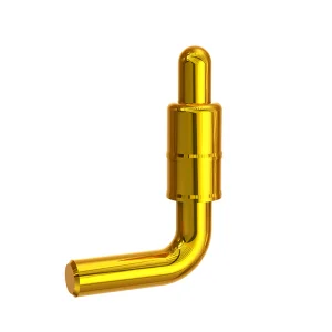
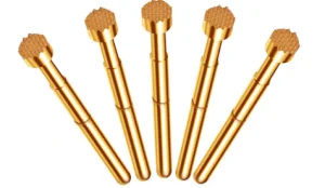
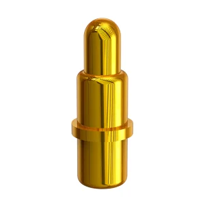
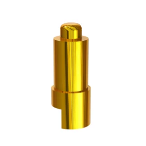
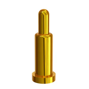
Engineered for high durability, low contact resistance, and exceptional coplanarity in electrical metrology and automated testing environments.
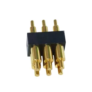
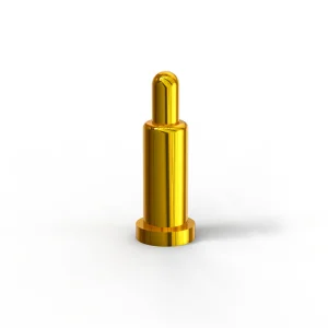
As integrated circuits scale down to sub-3nm nodes, wafer testing demands unmatched mechanical precision and electrical integrity. Wafer probes, working as the fundamental bridge between the Automated Test Equipment (ATE) and the silicon wafer, must transmit high-speed, high-density signals without damaging fragile metallization pads.
For silicon foundries, integrated device manufacturers (IDMs), and outsourced semiconductor assembly and test (OSAT) providers, probe card efficiency determines the overal Cost of Test (CoT) and final yield rates. Our customized wafer probing elements are optimized to minimize contact force, decrease contact resistance, and ensure stable performance over hundreds of thousands of touchdown cycles.
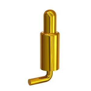
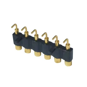
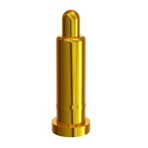
Whether you require vertical probes, cantilever pins, or custom pogo-style probe configurations for high-speed parametric testing, our advanced production floor utilizes high-grade materials and ultra-precise micro-machining tolerances to meet your packaging roadmap.
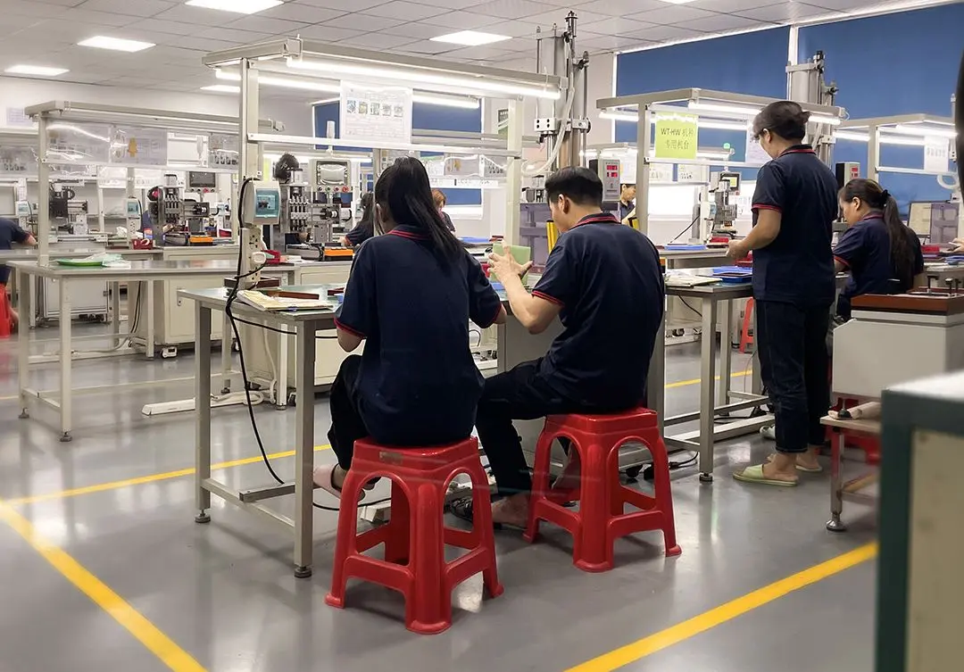
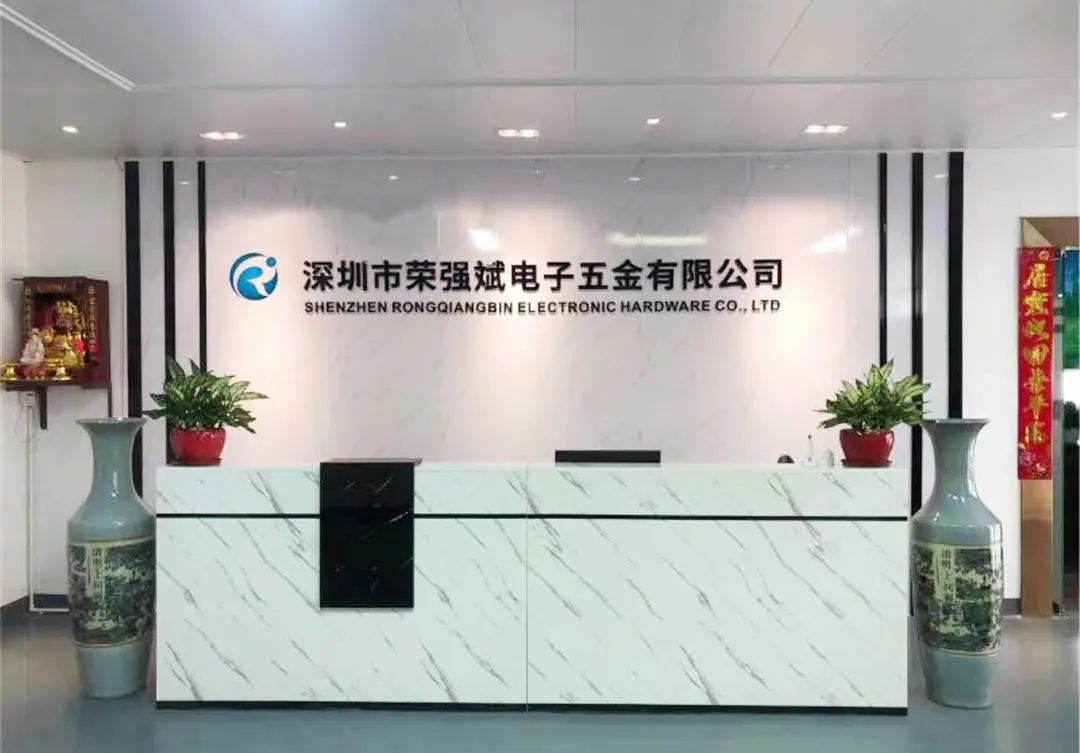

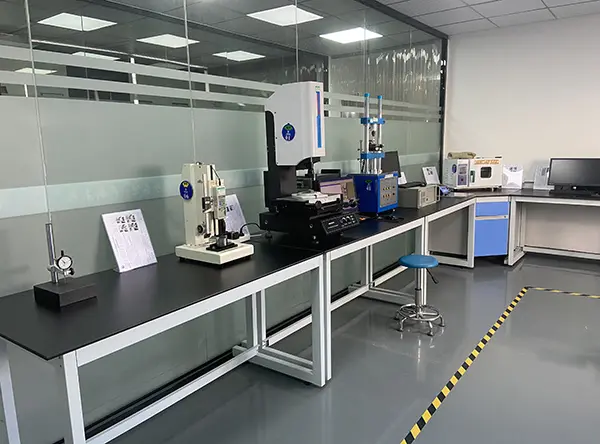
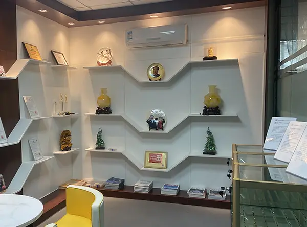
Founded in February 2011 in Songgang Street, Shenzhen—positioned within the high-tech hub of the Guangdong-Hong Kong-Macao Greater Bay Area—Shenzhen Rongqiangbin Electronic Hardware Co., Ltd. has established itself as an industry leader in POGO PIN micro-connector design and high-precision contact manufacturing.
Over a decade of manufacturing experience has allowed us to refine our spring contact technology, supplying to over 4,000 global clients and securing more than 300 active patents. Our technical engineering team excels in developing complex, ultra-fine-pitch testing pins and magnetic connectors that perform reliably under challenging thermal and mechanical conditions.
Under strict adherence to the ISO9001:2015 international quality management system, we maintain full in-house capabilities from design engineering to precise electroplating (including advanced gold-alloy finishes), assuring absolute compliance with international environmental standards.
Addressing the complex engineering challenges and strict specifications demanded by semiconductor procurement managers, OSATs, and test houses worldwide.
High-current wafer probe pins designed to sustain high current density and withstand extreme temperatures (-55°C to 175°C) during KGD (Known Good Die) testing of SiC and GaN MOSFETs.
State-of-the-art cantilever and vertical probe array structures designed for ultra-fine-pitch testing nodes, mitigating pad damage on high-performance compute chips (HPC) and complex SoC components.
Optimized RF wafer probes that minimize return loss (S11) and insertion loss (S21) up to 80 GHz, satisfying testing parameters for 5G transceivers, radar systems, and high-frequency communication modules.
To overcome physical scaling limits, our research and development programs focus heavily on material innovation. As modern dies utilize increasingly fragile Low-k dielectric layers, the probe's spring constant and tip shape must be engineered precisely to avoid surface cracking or interlayer delamination.
Our micro-probing contact tips are machined with premium alloys (such as Platinum-Nickel, Palladium-Copper, and heavily gold-plated Beryllium Copper) to offer structural rigidity alongside outstanding conductivity. This reduces particle accumulation (tip cleaning frequency) and extends probe card life cycle.
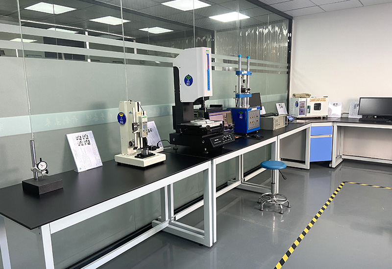

We believe in "Customer First, Integrity First." Our manufacturing pipeline is backed by a robust quality management system certified under ISO9001:2015. All micro-machined parts undergo meticulous optical measurement, spring-rate characterization, and electrical lifetime simulation.
For global trade security and environmental compliance, our entire catalog of contact systems complies with RoHS and REACH standards. We maintain complete material traceability, supplying certified test reports (including plating thickness validation via X-ray fluorescence) for every batch sent overseas.
Our commitment to excellence has earned us strategic partnership status with tier-one international enterprises, providing reliable test components for highly regulated consumer, automotive, and industrial applications.
Get professional answers regarding wafer testing probes, manufacturing capabilities, and customizable options.
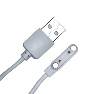
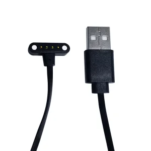
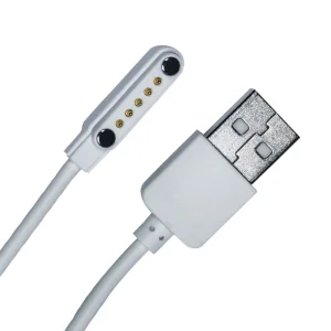
Explore our highly durable spring-loaded contacts and charging cables, engineered to meet strict international standards.
 Rongqiangbin Electronic