Engineered for extreme cyclical durability, minimized contact resistance, and maximum signal integrity in automated test equipment interfaces.
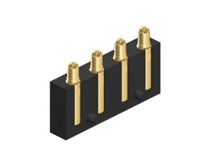
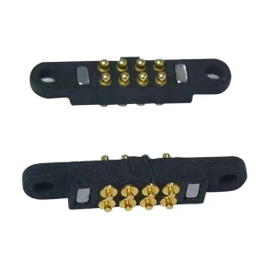
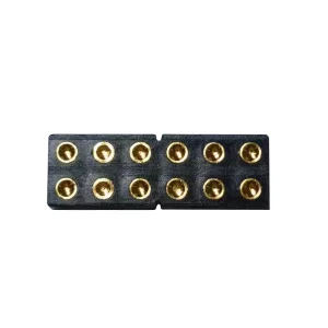
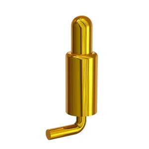
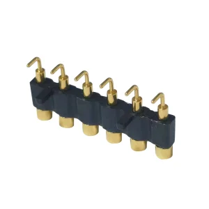
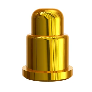
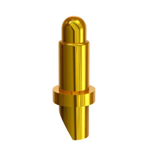
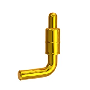
Analyzing the macro-technological transitions reshaping semiconductor validation interfaces, packaging demands, and test cycle efficiencies.
With the rise of Chiplets, System-in-Package (SiP), and 2.5D/3D integration, IC test sockets must support sub-0.3mm pitches, massive pin counts (often exceeding 5,000 pins per module), and delicate contact geometries that prevent silicon and pad deformation.
As 5G/6G systems and high-frequency radar modules proliferate, socket design is trending toward short electrical paths. Minimized self-inductance and capacitance are critical to support signal speeds exceeding 80 GHz with minimal insertion loss.
High-reliability sectors like automotive SoC and aerospace microprocessors demand validation across a extreme span of temperatures (-55°C to +175°C). Thermally optimized engineering materials and integrated heatsinks/heaters prevent thermal expansion variance.
Procurement departments in major semiconductor and ATE houses deal with multi-dimensional criteria when vetting potential ODM IC test socket factories. Speed to market, mechanical reliability, and structural yield stability are the cornerstones of volume optimization.
The socket must present ultra-low and extremely stable contact resistance (typically under 30 mΩ) over hundreds of thousands of actuation cycles to guarantee high yield rates.
During the chip prototype verification stage, test engineers need custom-engineered, application-specific sockets built and delivered within 1 to 2 weeks to stay on schedule.
By using custom high-end spring-loaded pins with wear-resistant plating, the cost per insertion is reduced, making large-scale production testing financially viable.
Aligning high-precision tooling manufacturing with critical electrical contact points to deliver robust hardware solutions.
Ideal for precision analog, power management ICs, and high-frequency RF systems. Separating the current path from the voltage measurement loop eliminates parasitic probe inductance and path resistance, yielding exact measurement dynamics.
Built with customized internal springs and ultra-thin barrels to allow standard grid array testing at pitches below 0.4mm. Ideal for mobile DRAM, CPU processors, and IoT system-on-chip modules.
Engineered for high current distribution and longevity during environmental screening. Employs thermal venting and highly conductive materials to handle continuous current runs without pin-tip degradation.
 RONGQIANGBIN
Founded in February 2011 on Songgang Street, Shenzhen, Shenzhen Rongqiangbin Electronic Hardware Co., Ltd. is located in the leading city of the Guangdong-Hong Kong-Macao Greater Bay Area. Over a decade of persistent development has enabled the company to grow into an industry leader, specialized in the engineering, customization, and manufacturing of premium Pogopin connectors and advanced test interface interfaces.
Operating under a strict philosophy of "customer first, integrity first," we maintain a highly specialized, technical production force focused on the complex demands of the POGO PIN and IC test socket component sectors.
Our production line has attained the ISO9001:2015 international quality management certification, supported by robust inspection workflows and complete environmental control compliance to supply high-reliability, eco-friendly connection products globally.
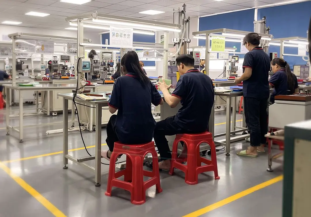

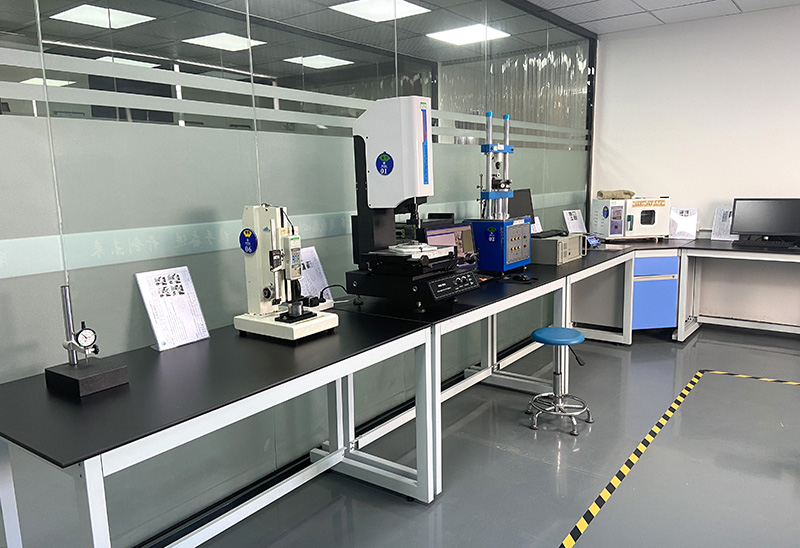
Since 2011, we have built custom solutions for over 4,000 global clients and secured more than 300 manufacturing patents.
Certified testing protocols integrated directly into production, backed by advanced instrumentation and 100% pre-shipment validation.
Optimized logistics networks and agile prototyping teams ensure swift project completion and prompt after-sales engineering response.
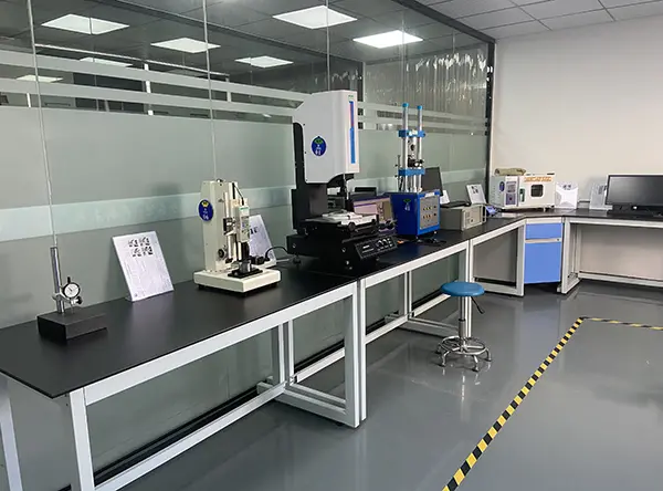
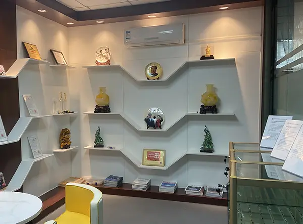
100% inspection during production stages and prior to custom batch dispatch.
How our factory is expanding precision engineering capabilities to meet next-generation chip testing standards.
Engineering custom spring probes with micro-diameters to match high-density chip packages and wafer-level test systems.
Developing short-path internal pin designs with tailored contact geometry to minimize inductance for optical and RF chips.
Deploying rhodium-ruthenium plating and custom-formulated cobalt alloys to prolong pin lifespan beyond 1,000,000 insertions.
Integrating micro-channel liquid cooling loops and localized thermistors into high-performance computing (HPC) test sockets.
For global chip designers and tier-1 system vendors, compliance and responsive technical support are critical. Our factory provides end-to-end design engineering capabilities alongside strict compliance frameworks.
Whether you need to test BGA, LGA, QFN, SOP, or customized sensors, our design team adapts contact configurations to match existing PCB footprint and ATE loadboard layouts.
Shenzhen, Guangdong, China
Serving global clients in Europe, Americas, and across APAC.
Expert responses addressing technical questions on IC test socket customization, pin configurations, and manufacturing capabilities.
To start custom engineering, we require the package datasheet (detailing dimensions, pitch, and pin patterns), chip package type (BGA, LGA, QFN, etc.), target test frequency, operational temperature range, and preferred actuation mechanism (clamshell, open-top, or automated handler compatibility).
We control signal integrity by reducing the electrical path length of our spring-loaded contact pins, implementing coaxial shield structures, and running extensive HFSS simulation profiles to achieve insertion loss (S21) levels below 1dB at up to 80 GHz.
Our standard pogo pins achieve 100,000 to 500,000 cycles under typical operation. By applying specialized gold alloy plating and precision surface processing, we can achieve lifespans exceeding 1,000,000 cycles for automated test systems.
Yes, our design team routinely integrates top-side heat sink mounts, custom heat pipes, thermal ventilation chambers, and localized heater cartridges inside the socket assembly, protecting the chip and the socket during high-power burn-in cycles.
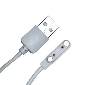
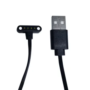
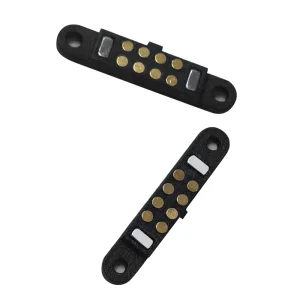
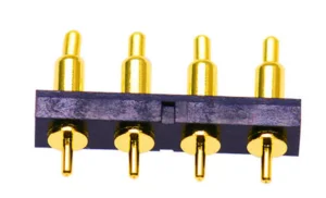
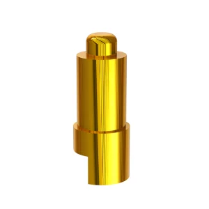
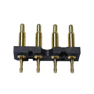
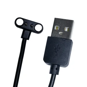
Further options for custom connectors, magnetic charging assemblies, and specialized testing spring contacts.
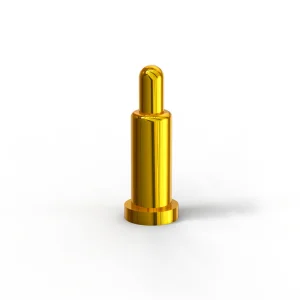
 Rongqiangbin Electronic