As microelectronics shrink down to single-digit nanometer processes, traditional testing approaches have become a bottleneck. Under the demands of Wafer-Level Chip-Scale Packaging (WLCSP) and Known Good Die (KGD) requirements, finding physical testing anomalies before final packaging has become critical to preventing expensive failure rates in subsequent assembly stages.
Custom wafer-level testing bridges the gap between raw wafer fab runs and highly integrated systems-in-package (SiP). By deploying high-precision spring-loaded probe structures and customized test socket adapters, manufacturers verify structural integrity, electrical performance, and high-speed signal pathways directly on the silicon wafer. This level of quality verification demands hardware interfaces that can maintain coplanarity across thousands of contact points under complex thermal environments.
A failed die packaged into a multi-chip module ruins the entire assembly. For modern AI and automotive chips, attaining a Zero Defect Rate is standard procedure. Achieving this goal requires specialized contact interfaces that offer:
Analyzing international demand waves across the Americas, EMEA, and Asia-Pacific regions for micro-contact testing hardware.
Automotive grade microcontrollers and power management ICs must endure extreme thermal cycles ranging from -40°C to 150°C. Sourcing teams prioritize wafer test interface suppliers that can demonstrate material reliability at temperature extremes, ensuring probe alignment and contact force stability do not deteriorate during hot and cold test stages.
Next-generation server and computing chips operate on high frequency lines and pull massive current profiles. This demands custom contact structures (like advanced pogo-pin blocks and vertical probe substrates) capable of delivering low parasitic inductance, high bandwidth limits, and current carrying capacities reaching up to 1.5A per pin.
The push for smaller profiles requires extremely tight probe pitch requirements (down to 150 µm or lower). Procurement departments seek customized adapter factories that offer fast lead times, rapid prototyping, and high consistency in mass fabrication of spring probe configurations.
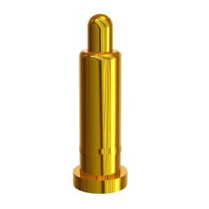
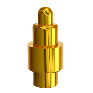
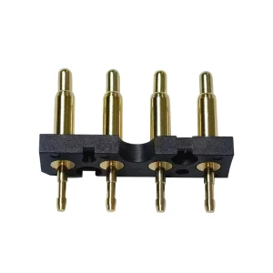
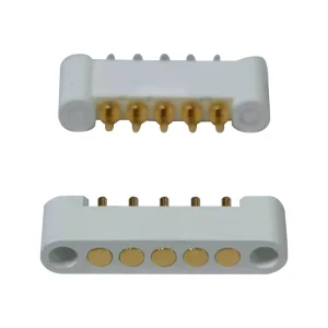
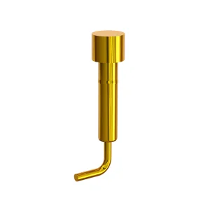
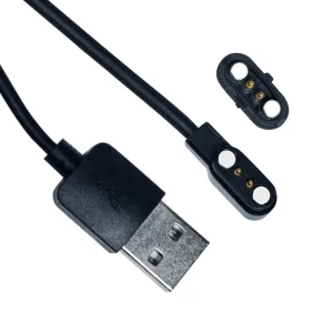
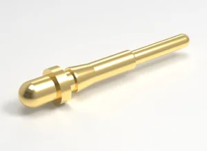
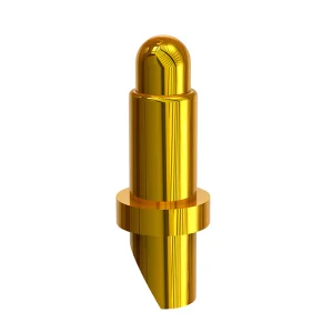
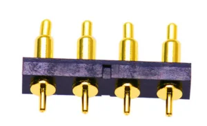
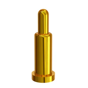
To successfully run high-throughput testing, probe cards must be connected to the Automated Test Equipment (ATE) through high-density interfaces. This is where custom-engineered spring contact probes (Pogo Pins) and advanced socket frames play a critical role.
At Rongqiangbin (RQB), our mechanical designs optimize three main performance attributes:
Designing interface hardware for semiconductor wafer testing requires strict manufacturing capabilities. The micro-pitch dimensions involved mean that minor design variations can cause probe misalignment or unstable contact, leading to false yield failures in costly silicon wafers.
Our production facilities utilize automated CNC micro-machining, clean-room assembly lines, and high-speed electrical characterization tools. We collaborate closely with probe card designers to supply precision DIP socket pins, SMT/SMD spring probes, and robust housing blocks that sit at the core of advanced ATE wafer interfaces.
Solving the technical friction points between packaging design and high-volume test manufacturing floor operations.
As temperatures rise during test routines, thermal expansion can shift probe locations away from wafer pads. RQB uses low-CTE (Coefficient of Thermal Expansion) ceramic and alloy elements within our pin housings to ensure placement accuracy within ±5 µm.
Longer-lasting contact probes reduce replacement downtime. Our customized gold-alloy plating formulations minimize wafer solder adherence, reducing cleaning cycles from every 10,000 touches to over 50,000 touches, maximizing machine utilization.
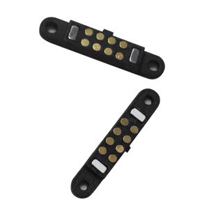
Modern mixed-signal wafers require power lines alongside sensitive signal channels. We construct hybrid contact blocks that integrate heavy-current power pins together with coaxial high-frequency pins in one compact, unified form factor.
Keeping pace with advanced semiconductor development: 2.5D/3D packaging, heterogeneous chip integration, and sub-100um pitch challenges.
The semiconductor industry is moving rapidly toward heterogeneous integration, stacking chiplets using silicon via (TSV) techniques. Testing these micro-stack structures before packaging presents a significant engineering challenge. The contact pitch is dropping below 100 micrometers, requiring probe pins that are smaller than a human hair.
To support this roadmap, RQB's research and development focus is centered on:
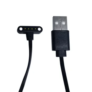
Founded in February 2011 in Songgang Street, Shenzhen, within the Guangdong-Hong Kong-Macao Greater Bay Area, Shenzhen Rongqiangbin Electronic Hardware Co., Ltd. (RQB) specializes in the engineering, design, and manufacturing of high-reliability Pogo Pin connectors, spring-loaded probes, and custom testing socket interfaces.
Over more than a decade of steady growth, we have expanded to become an industry leader, operating advanced production facilities and earning ISO 9001:2015 certification for our quality management systems. Our strong technical team works closely with clients to deliver high-performance contact interfaces that meet strict mechanical and environmental standards.
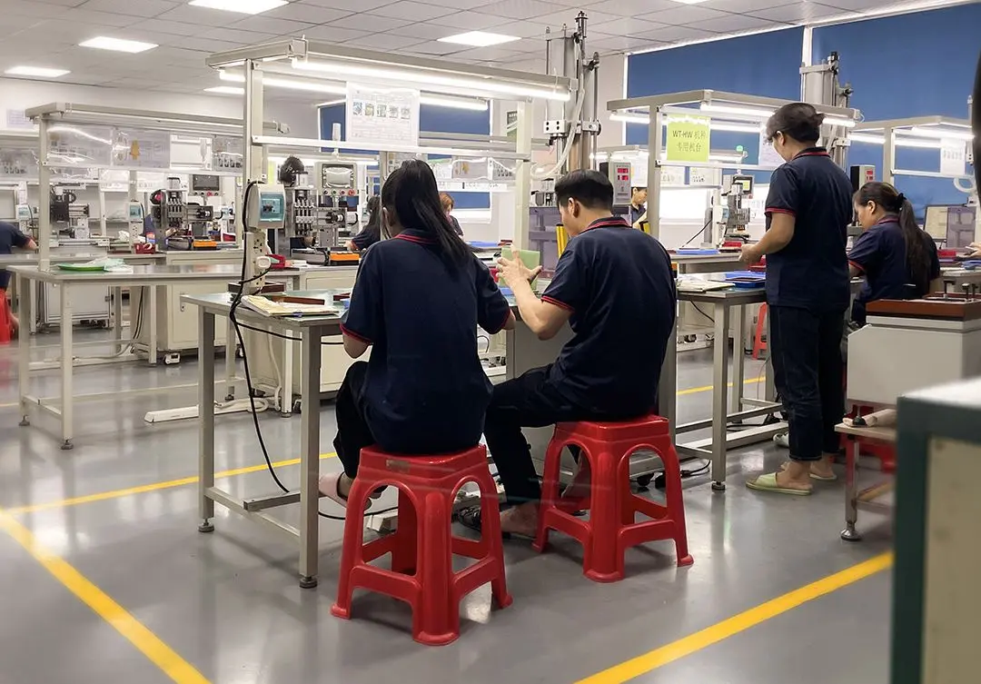
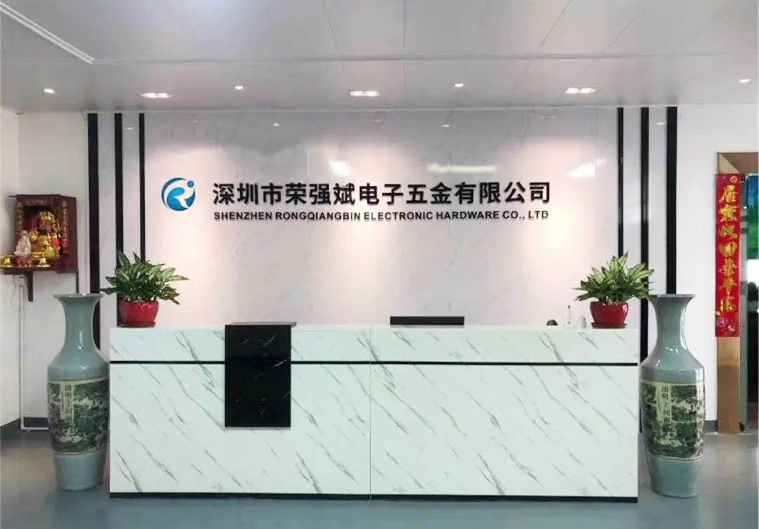

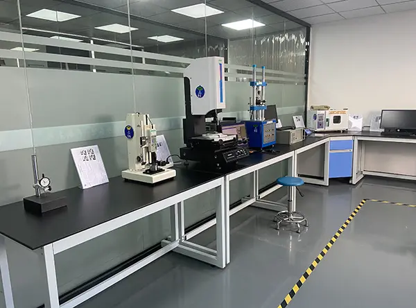
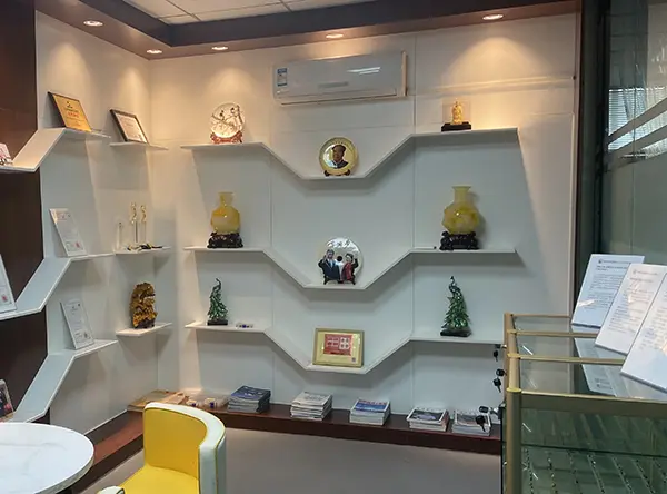
We partner with premier technology and automotive brands to provide reliable contact and hardware connection systems.
Shenzhen Rongqiangbin operates under strict quality management structures. Our manufacturing line processes are certified to the ISO 9001:2015 standard, which governs everything from raw material verification to final optical inspections of our spring probes and custom test sockets.
Additionally, we comply with RoHS and REACH standards to meet international environmental regulations. Our engineering team assists with full compliance documentation, test reports, and metallurgical analyses to streamline your internal audits.
We understand that wafer-level test hardware development requires prompt, detailed technical support. Our engineering offices provide fast turnarounds for technical design files, 3D CAD modeling, and FEA simulation feedback, helping you keep your test programs on schedule.
Whether you are upgrading an existing vertical probe assembly, developing custom test adapters, or sourcing high-durability spring contact pins, RQB provides reliable manufacturing capability and technical expertise.
Frequently asked engineering questions regarding probe interfaces, spring pins, and manufacturing capabilities.
Our standard manufacturing processes support pin array pitches down to 0.4mm using conventional spring probe architectures. For micro-pitch needs below 0.35mm, we utilize specialized guide plates and thin-profile plunger structures. We also collaborate with probe card houses on custom micro-machined blocks designed to align with sub-100µm structures.
We apply specialized coatings to the probe tips, such as hard gold alloys or proprietary platinum-group finishes. These materials reduce the affinity for tin oxide pickup from wafer bumps, minimizing residue buildup. This extends cleaning intervals, lowers maintenance downtime, and helps keep contact resistance stable throughout high-volume test runs.
We subject our test probes and sockets to 100% mechanical inspection. This includes dimensional checks with high-resolution optical comparator systems, spring-force calibration, and contact resistance verification. In addition, we conduct life-cycle testing and environmental stress screening (ESS) to confirm long-term mechanical and electrical stability.
Yes. We manufacture customized connection systems using customer-supplied drawings. Our team accepts SolidWorks, AutoCAD, and STEP files, and our engineers review your layouts to optimize the design for manufacturability (DFM). This collaborative process helps verify mechanical tolerances and signal performance requirements prior to production.
We select materials with low coefficients of thermal expansion (CTE) for our housing blocks and match the spring tension to counteract the thermal changes. This ensures that the probe pins stay centered on the wafer pads even at test temperatures up to 150°C, preventing alignment shifts and wafer damage.
 Rongqiangbin Electronic