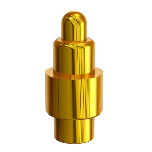
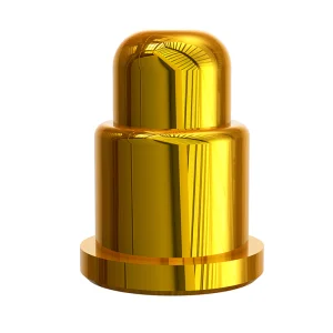
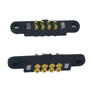
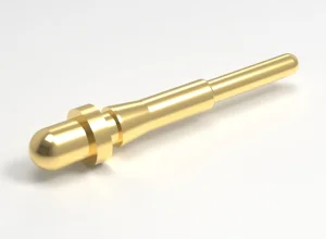
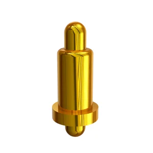
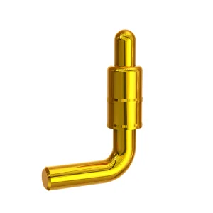
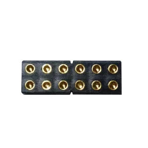
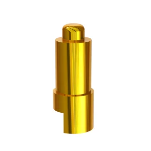
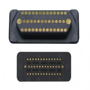
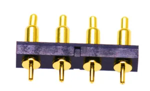
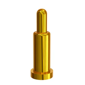
High-durability interfaces optimized for advanced electrical testing, device burn-in, and probe applications.
The wafer probe testing process serves as the gatekeeper of silicon yield in modern semiconductor manufacturing. Conducted during the front-end-of-line (FEOL) and back-end-of-line (BEOL) transitions, this critical stage involves electrical testing of individual dies (known as wafer sorting or wafer testing) while they are still in wafer form. By identifying and isolating defective dies prior to the expensive packaging phase, wafer probing directly impacts structural fab yield and dramatically reduces total packaging and test costs. The core engineering challenge lies in establishing reliable, repeatable, and low-resistance physical contact with sub-micron wafer pads (aluminum or copper bumps) without causing mechanical damage to the underlying silicon structures.
Through advanced Automatic Test Equipment (ATE), micro-positioning wafer probers align a wafer to a specialized probe card. This card contains arrays of miniature probe pins—specifically engineered pogo pins, cantilever probes, or vertical spring-loaded probes—which physical compress onto the die's contact pads. Power, ground, and high-frequency digital/RF signals are routed through these interfaces to diagnose electrical performance under extreme operational variations, including high temperatures (up to 150°C) and low thermal thresholds.
At the center of the wafer probe testing interface is the Probe Card, which serves as the physical and electrical translation layer between the massive, high-pin-count tester and the microscopic dimensions of the silicon wafer. Achieving stable electrical contacts across thousands of dense micro-pads simultaneously requires mechanical precision at the micron level. This is where spring-loaded contacts (Pogo Pins) play a critical role. Unlike cantilever probes, spring-loaded pogo pins offer vertical compliance, compensating for wafer planarity deviations and guaranteeing uniform contact force across the entire die array.
Advanced spring-loaded pins maintain a stable Cres (typically < 50 mΩ) under minimal force to prevent signal degradation and wafer pad indentation.
Tailored probe designs and materials maintain high-bandwidth signal integrity up to 40 GHz, crucial for testing 5G transceivers and high-speed processors.
Precision internal engineering allows the pins to endure over 500,000 to 1,000,000 compression cycles without experiencing mechanical fatigue or spring failure.
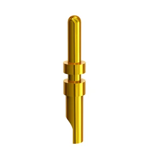
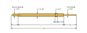
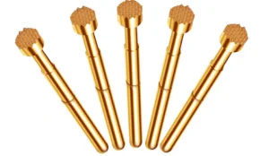
Key parameters in pogo pin design for wafer probe card interfaces include barrel geometry, spring rate, plunger tip design (e.g., crown, 4-point, pointed, or flat), and electroplating materials. Heavy gold (Au) or palladium-cobalt (PdCo) plating is typically applied to prevent probe oxidation and reduce tip contamination, allowing for extended test cycles between cleaning intervals.
Procurement departments in global semiconductor giants, OSAT (Outsourced Semiconductor Assembly and Test) providers, and consumer electronics brands face intense challenges when sourcing high-precision probe hardware. With wafer geometry shrinking down to sub-3nm nodes, testing demands have shifted from standard pitch components to ultra-fine-pitch, customized vertical probe card blocks.
As the semiconductor industry advances toward heterogeneous integration (such as chiplets and High Bandwidth Memory - HBM3/HBM4), testing complexity scales non-linearly. The technological roadmap for wafer probing processes focuses on three primary vectors: pitch reduction, thermal performance, and high-frequency capabilities.
Micro-bump arrays in advanced packaging necessitate probe pins with diameters under 50μm. Designing internal spring mechanisms at this scale requires highly advanced alloy metallurgy, shifting from traditional beryllium copper (BeCu) to custom tungsten/cobalt alloys to retain tensile strength and conductivity. Additionally, testing high-performance computing (HPC) and AI accelerators requires high current densities, with probe pins needing to support up to 3A of continuous current per pin without experiencing thermal runaway.
The applications for custom spring-loaded connections and probe testing interfaces span critical modern technology verticals, each requiring specialized material properties and mechanical tolerances.
Requires extreme high-temperature stability (tested up to 150°C) and resistance to physical vibrations. Pogo pin systems in burn-in and wafer sort must ensure zero latent defects for safety-critical ADAS chips.
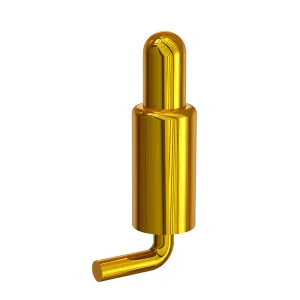
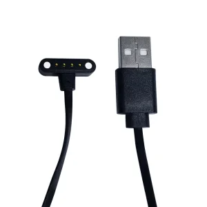
Focuses on miniature designs, waterproof features (IP67/IP68), and reliable plating to resist sweat corrosion. Double-headed and bending type pogo pins are widely used in Bluetooth headphone docks and magnetic data transfer links.
Requires high-current charging pins and robust connectors capable of handling high voltages and rapid thermal transfers. Customized NEV pin chargers ensure long-term charging cycle reliability.
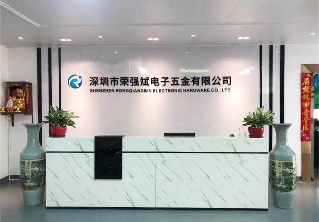
Shenzhen Rongqiangbin Electronic Hardware Co., Ltd. is located in Shenzhen, the leading city of the Guangdong-Hong Kong-Macao Greater Bay Area. Founded in February 2011 on Songgang Street, Shenzhen, we specialize in the development and manufacturing of high-quality Pogo Pin connectors, spring-loaded contacts, and customized testing probes. After years of dedicated effort, precision engineering, and technological advancements, our company has become a leader in the precision connector industry.
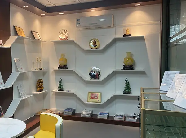
Driven by the core values of "customer first, integrity first," we boast an expert technology production team. We have established long-term cooperative partnerships with numerous world-renowned brands. Our company is certified under the ISO9001:2015 international quality management system, and we feature a strong quality assurance team and environmental management systems to supply high-reliability, environmentally compliant products globally.


Our Major Global Partners & Clients:
Shenzhen Rongqiangbin implements strict quality standards at every stage of the manufacturing process. From raw material input to the final shipment of our spring-loaded pins, our QA teams enforce strict inspection standards to guarantee compatibility and performance.
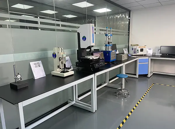
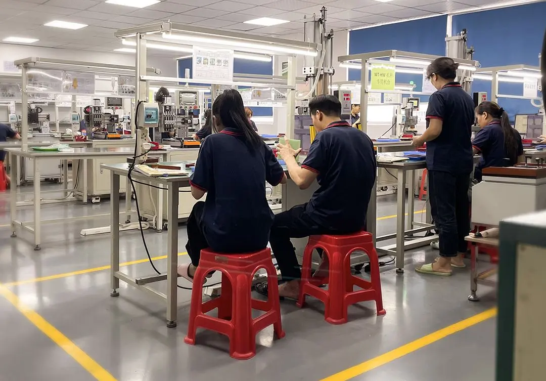
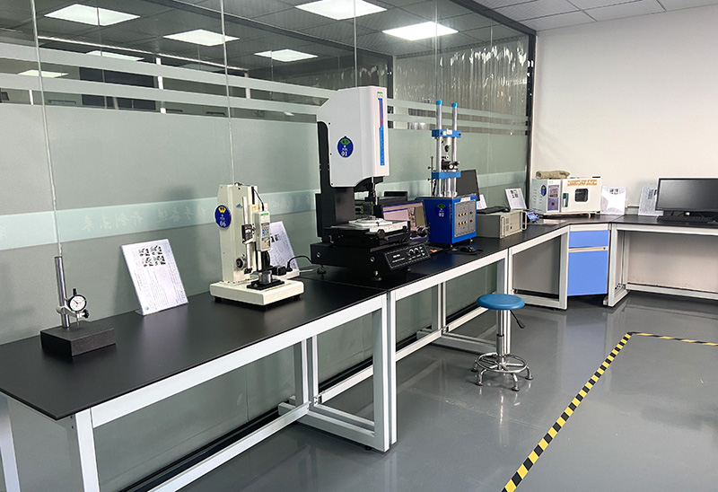
Operating out of a highly modernized manufacturing plant, we run automated optical inspection (AOI) lines, dynamic resistance testers, and micro-force measurement systems. By conducting continuous testing across thousands of physical compression cycles, we provide our clients with detailed test logs and certificate packets to guarantee that every batch of products meets high industrial standards.
Expert technical insights on wafer probing processes, pogo pin selections, and custom specifications.
Explore our collection of custom charging and signal transmission connectors, designed for automotive, wearable, and industrial applications.
 Rongqiangbin Electronic