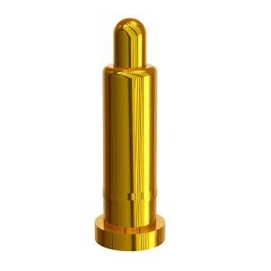
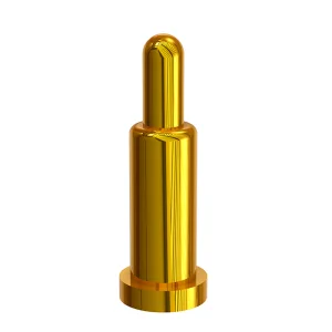
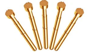
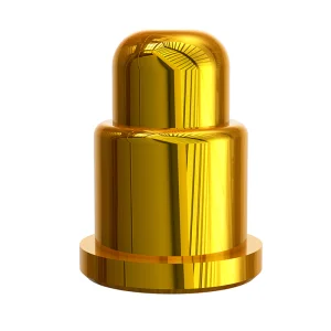
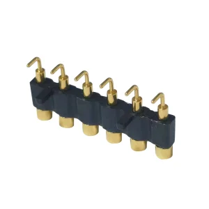
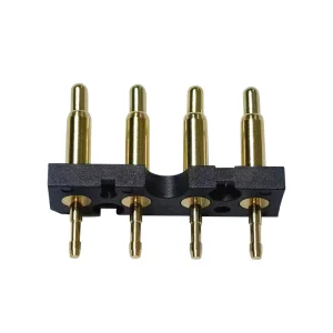
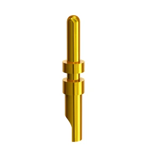
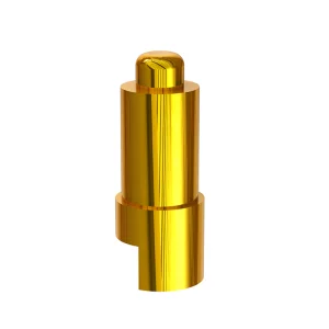
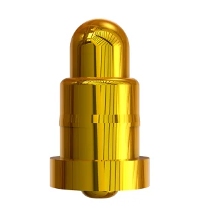
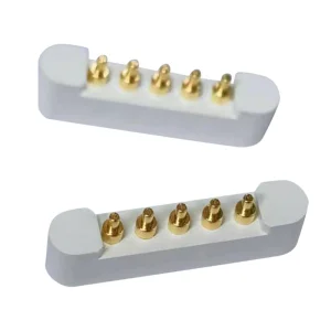
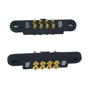
Explore our leading OEM/ODM customized pogo pins and spring probe interfaces.
Industrial intelligence and micro-electrical demand driving the evolution of advanced contact probes.
In today's highly dynamic microelectronics and semiconductor manufacturing ecosystems, the term "Probe S" (encompassing specialized spring-loaded test probes, semiconductor wafer contact pins, and custom pogo interface configurations) represents the crucial touchpoint between silicon architecture and testing interfaces. Over the last decade, as microprocessors transitioned to sub-3nm nodes and consumer electronics embraced ultra-slim profiles with multi-functional capabilities, the global demand for precision micro-contacts has grown exponentially. As a dedicated OEM Probe S manufacturer and factory, our role has evolved from a simple component maker to a strategic design partner facilitating zero-defect manufacturing.
The commercial deployment of these spring probes is visible across highly critical sectors, including aerospace instrumentation, smart industrial automation, automotive electronics, and ultra-high-speed consumer telecommunications. With the emergence of advanced driver-assistance systems (ADAS) in Electric Vehicles (EVs) and the rolling deployment of 5G/6G network terminals, spring contact probes are exposed to increasingly hostile operational environments. They must deliver high current carrying capacities (up to 15A or higher in power applications), sustain millions of cycle compressions without structural decay, and maintain exceptionally low contact resistance (<20mΩ).
Geographically, the manufacturing footprint of high-end spring-loaded contacts is concentrated in precision engineering hubs. Among them, the Shenzhen-Dongguan corridor within the Guangdong-Hong Kong-Macao Greater Bay Area has established itself as the global epicenter for industrial connector and spring probe manufacturing. This concentration offers unparalleled supply chain agility, enabling factories to source raw alloys (such as beryllium copper, phosphor bronze, and high-purity stainless steel) and execute state-of-the-art electroplating processes (ranging from standard gold plating to advanced palladium-nickel barrier layers) at unmatched speed and efficiency.
Inside the microscopic engineering of high-reliability spring contact systems.
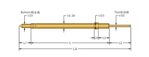
The mechanical architecture of a high-performance spring contact probe comprises three core components: the plunger, the barrel, and the internal spring. Each element must be designed with precise structural integrity to achieve optimal electrical conductivity and mechanical endurance.
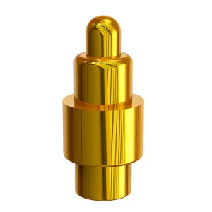
Plungers are precision turned from beryllium copper (BeCu) or tool steel (SK4) to maximize hardness. They are plated with thick layers of gold (Au) or Platinum-group alloys to guarantee minimum contact resistance and high corrosion resistance, even under harsh chemical exposure.
Springs are coiled from music wire (SWP) or stainless steel (SUS) to ensure constant force profiles over life cycles exceeding 1,000,000 compressions. Precision pre-loads prevent signal degradation due to contact chatter or physical vibrations.
Barrels are engineered as seamless, deep-drawn brass tubes to prevent lateral friction inside the guide plate. The inner surfaces are polished and gold-plated to ensure smooth mechanical sliding and steady contact resistance values.
To address signal integrity at high frequencies (exceeding 20 GHz in RF testing), the contact geometry must be carefully optimized. Engineers use Finite Element Analysis (FEA) to simulate electromagnetic fields and minimize insertion loss and return loss. The plating must also be formulated to prevent solder migration and tin-whiskering, which are leading causes of contact failure in automated SMT manufacturing lines.
How spring probes bridge structural gaps across multiple industrial domains.
Spring contact probes are highly adaptable, making them invaluable across diverse application environments. Below are the key scenarios where custom OEM Probe S implementations are vital:
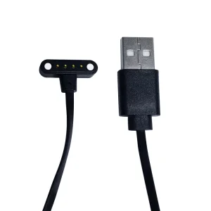
With smartwatches and TWS earbuds requiring waterproof protection (IP68), traditional charging ports are replaced by gold-plated SMT/SMD pogo pins. These contacts resist human sweat corrosion and guarantee secure charging interfaces in space-constrained enclosures.
Modern vehicles employ spring-loaded contacts for sensor hubs, infotainment systems, and high-voltage battery management systems. They endure high vibrations and extreme thermal cycles (-40°C to +125°C) while maintaining continuous electrical connectivity.
IC testing demands ultra-fine pitch probes (down to 0.2mm pitch) to inspect Wafer-Level Chip-Scale Packages (WLCSP). Our specialized manufacturing techniques produce micro-probes with tight physical tolerances (+/-0.01mm) to prevent pad damage on silicon wafers.
For smart factories embracing Industry 4.0, spring contact probes play a key role in automated testing equipment (ATE). By integrating customized probe interfaces into automated pick-and-place lines, factories can run 100% in-line electrical testing for every PCB produced, virtually eliminating field failures and optimizing overall manufacturing yields.
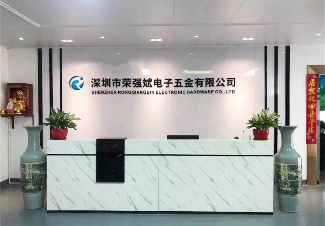
Shenzhen Rongqiangbin Electronic Hardware Co., Ltd.
Founded in February 2011 in Songgang Street, Shenzhen, Shenzhen Rongqiangbin Electronic Hardware Co., Ltd. is located at the center of the Guangdong-Hong Kong-Macao Greater Bay Area. Over years of focused effort, our company has become a leader in the development, engineering, and manufacturing of high-quality Pogo pin connectors and precision hardware.
Guided by our core principles of "customer first, integrity first," we have built a highly skilled technical team and established long-term partnerships with leading companies worldwide. Backed by our ISO9001:2015 quality management system certification, we implement rigorous quality and environmental controls to ensure all products comply with environmental regulations (including RoHS and REACH).
Our Tier-1 Client Portfolio includes: Honeywell, Samsung, SIEMENS AG, ZTE, 360, QCY, HAYLOU, Shanghai Laimu, Luxshare Group, Aoni Electronics, and Amphenol Group.
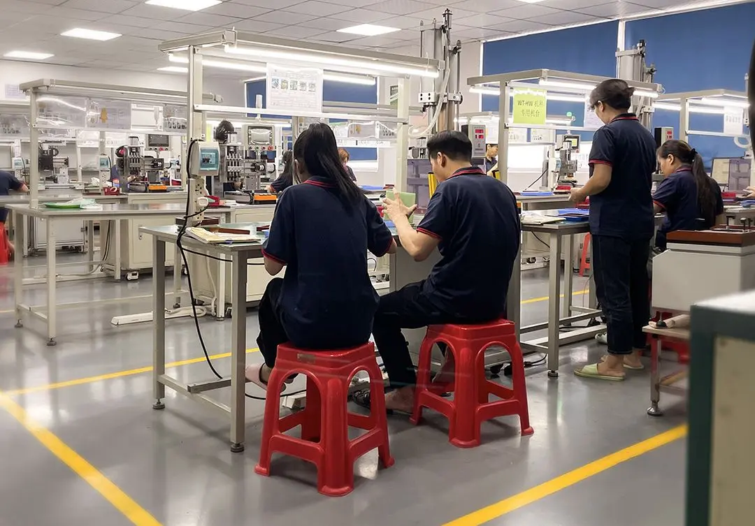

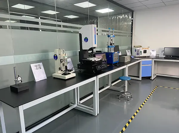
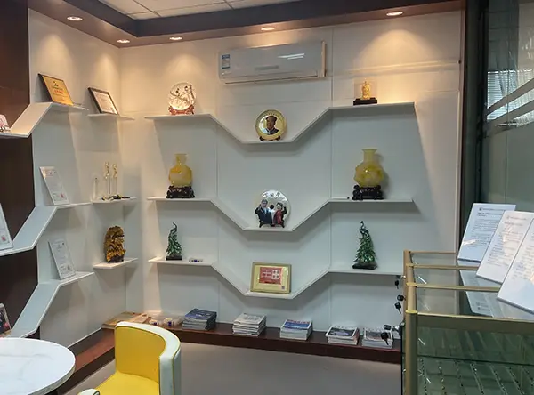
Our Core Strengths & Industry Advantages
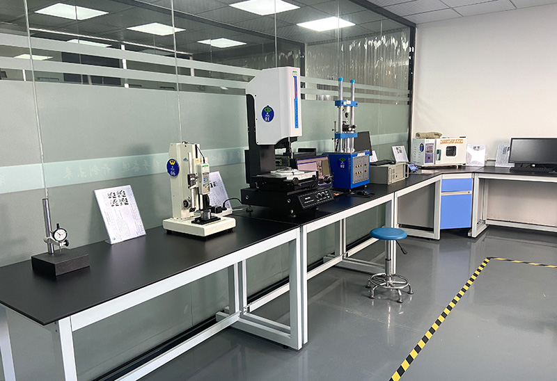

"Committed to being an excellent POGO PIN manufacturer recognized for outstanding quality and cost-effectiveness both domestically and abroad, while driving the development of advanced connector technologies."
Expert insights on metallurgy, tolerances, and design requirements for engineering teams.
Engineered to meet rigorous tolerances for advanced industrial applications.
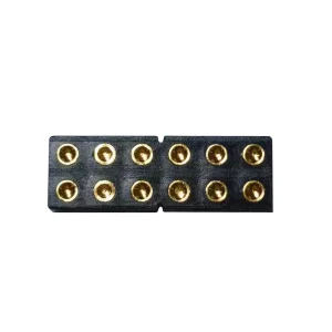
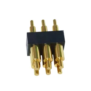
 Rongqiangbin Electronic